计算机系统要素
1 布尔逻辑
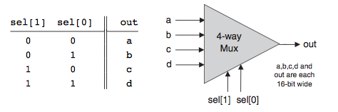
多通道/多位Multiplexor:
一个拥有m个通道、每个通道数据宽度为n位的多路复用器(multiplexor),将m个n位输入变量中选择一个并从其单一的n位输出总线上输出。可以用k个控制位来指定这个选择k=\log_2m。
例:4通道16位的multiplexor(4-way Multiplexor):
多通道/多位Demultiplexer: m通道、n位的Demultiplexer从m个可能的n位输出通道中选择一个n位的输入变量。可以用k个控制位来指定这个选择k=\log_2m。
例:4-way Demultiplexer:
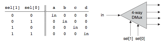
/**
 * 4-way demultiplexer:
 * {a, b, c, d} = {in, 0, 0, 0} if sel == 00
 *                {0, in, 0, 0} if sel == 01
 *                {0, 0, in, 0} if sel == 10
 *                {0, 0, 0, in} if sel == 11
 */

CHIP DMux4Way {
    IN in, sel[2];
    OUT a, b, c, d;

    PARTS:
    DMux(in=in, sel=sel[1], a=c1, b=c2);
    DMux(in=c1, sel=sel[0], a=a, b=b);
    DMux(in=c2, sel=sel[0], a=c, b=d);

}
2 布尔运算
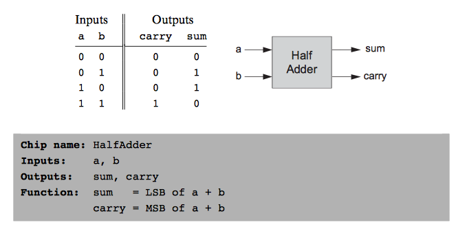
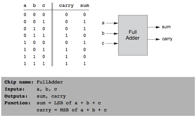
半加器(Half Adder): 进行二进制数加法的第一步就是要能够对两个二进制位进行相加。这里把结果的LSB(Least Significant Bit)称为sum,MSB(Most Significant Bit)称为carry。
HDL语言:
CHIP HalfAdder {
    IN a, b;    // 1-bit inputs
    OUT sum,    // Right bit of a + b
        carry;  // Left bit of a + b

    PARTS:
    And(a=a, b=b, out=carry);
    Xor(a=a, b=b, out=sum);
}
全加器:用来对三个位相加。
HDL 语言:
CHIP FullAdder {
    IN a, b, c;  // 1-bit inputs
    OUT sum,     // Right bit of a + b + c
        carry;   // Left bit of a + b + c

    PARTS:
    HalfAdder(a=a, b=b, sum=sum1, carry=carry1);
    HalfAdder(a=c, b=sum1, sum=sum, carry=carry2);
    Or(a=carry1, b=carry2, out=carry);
}
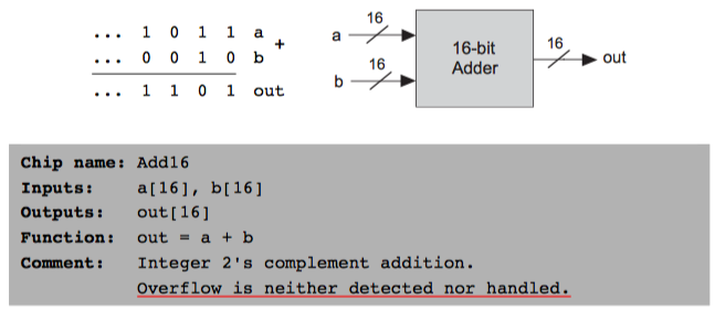
加法器(Adder): 存储器和寄存器电路用n位的形式来表示整数,n可以是16、32、64等等, 这依赖于所在的计算机平台。进行n位加法的芯片称为多位加法器(multi-bit adder),或者简称为加法器。下图为16位加法器
HDL:
CHIP Add16 {
    IN a[16], b[16];
    OUT out[16];

    PARTS:
   HalfAdder(a=a[0], b=b[0], carry=carry1, sum=out[0]);
   FullAdder(a=a[1], b=b[1], c=carry1, carry=carry2, sum=out[1]);
   FullAdder(a=a[2], b=b[2], c=carry2, carry=carry3, sum=out[2]);
   FullAdder(a=a[3], b=b[3], c=carry3, carry=carry4, sum=out[3]);
   FullAdder(a=a[4], b=b[4], c=carry4, carry=carry5, sum=out[4]);
   FullAdder(a=a[5], b=b[5], c=carry5, carry=carry6, sum=out[5]);
   FullAdder(a=a[6], b=b[6], c=carry6, carry=carry7, sum=out[6]);
   FullAdder(a=a[7], b=b[7], c=carry7, carry=carry8, sum=out[7]);
   FullAdder(a=a[8], b=b[8], c=carry8, carry=carry9, sum=out[8]);
   FullAdder(a=a[9], b=b[9], c=carry9, carry=carry10, sum=out[9]);
   FullAdder(a=a[10], b=b[10], c=carry10, carry=carry11, sum=out[10]);
   FullAdder(a=a[11], b=b[11], c=carry11, carry=carry12, sum=out[11]);
   FullAdder(a=a[12], b=b[12], c=carry12, carry=carry13, sum=out[12]);
   FullAdder(a=a[13], b=b[13], c=carry13, carry=carry14, sum=out[13]);
   FullAdder(a=a[14], b=b[14], c=carry14, carry=carry15, sum=out[14]);
   FullAdder(a=a[15], b=b[15], c=carry15, carry=carry, sum=out[15]);

}
算数逻辑单元(Arithmetic Logic Unit, ALU): 计算一组固定的函数out=f_i(x,y),这里x和y是芯片的两个16位输入,out是芯片的16位输出, f_i是位于一个函数表中的函数,该函数表通过6个控制位(control bit)的输入位(zx, nx, zy, ny, f, no)来告诉ALU用哪一个函数来进行何种计算。
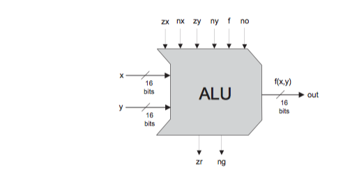
HDL:
*
 * The ALU (Arithmetic Logic Unit).
 * Computes one of the following functions:
 * x+y, x-y, y-x, 0, 1, -1, x, y, -x, -y, !x, !y,
 * x+1, y+1, x-1, y-1, x&y, x|y on two 16-bit inputs,
 * according to 6 input bits denoted zx,nx,zy,ny,f,no.
 * In addition, the ALU computes two 1-bit outputs:
 * if the ALU output == 0, zr is set to 1; otherwise zr is set to 0;
 * if the ALU output < 0, ng is set to 1; otherwise ng is set to 0.
 */

// Implementation: the ALU logic manipulates the x and y inputs
// and operates on the resulting values, as follows:
// if (zx == 1) set x = 0        // 16-bit constant
// if (nx == 1) set x = !x       // bitwise not
// if (zy == 1) set y = 0        // 16-bit constant
// if (ny == 1) set y = !y       // bitwise not
// if (f == 1)  set out = x + y  // integer 2's complement addition
// if (f == 0)  set out = x & y  // bitwise and
// if (no == 1) set out = !out   // bitwise not
// if (out == 0) set zr = 1
// if (out < 0) set ng = 1

CHIP ALU {
    IN
        x[16], y[16],  // 16-bit inputs
        zx, // zero the x input?
        nx, // negate the x input?
        zy, // zero the y input?
        ny, // negate the y input?
        f,  // compute out = x + y (if 1) or x & y (if 0)
        no; // negate the out output?

    OUT
        out[16], // 16-bit output
        zr, // 1 if (out == 0), 0 otherwise
        ng; // 1 if (out < 0),  0 otherwise

    PARTS:
    // if (zx==1) set x = 0
    Mux16(a=x,b=false,sel=zx,out=zxout);

    // if (zy==1) set y = 0
    Mux16(a=y,b=false,sel=zy,out=zyout);

    // if (nx==1) set x = ~x
    // if (ny==1) set y = ~y
    Not16(in=zxout,out=notx);
    Not16(in=zyout,out=noty);
    Mux16(a=zxout,b=notx,sel=nx,out=nxout);
    Mux16(a=zyout,b=noty,sel=ny,out=nyout);

    // if (f==1)  set out = x + y
    // if (f==0)  set out = x & y
    Add16(a=nxout,b=nyout,out=addout);
    And16(a=nxout,b=nyout,out=andout);
    Mux16(a=andout,b=addout,sel=f,out=fout);

    // if (no==1) set out = ~out
    // 1 if (out<0),  0 otherwise
    Not16(in=fout,out=nfout);
    Mux16(a=fout,b=nfout,sel=no,out=out,out[0..7]=zr1,out[8..15]=zr2,out[15]=ng);

    //if (out==0), zr=1
    Or8Way(in=zr1,out=or1);
    Or8Way(in=zr2,out=or2);
    Or(a=or1,b=or2,out=or3);
    Not(in=or3,out=zr);

}
3 时序逻辑
时钟(Clock):在大多数计算机里,时间的流逝是用主时钟(master clock)来表示的,它提供连续的交变信号序列。其精确的硬件实现通常基于振荡器(oscillator), 其在两个信号值0-1之间交替变化。两个响铃的时间间隔称为时钟的周期。
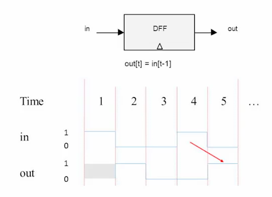
触发器(Flip-Flop): 计算机里最基本的时序单元,有多个变种。数据触发器(Data Flip-Flop, DFF),其接口包含1比特位输入和1比特位输出。 DFF简单地将前一个时间周期的输入值作为当前周期的输出。
寄存器(Registers): 具有记忆功能的设备,能"存储"某一时刻的值,实现经典的存储行为out(t)=out(t-1)。从另一个方面来说,DFF仅能够输出它前一时钟周期的输入,也就是out(t)=in(t-1)。寄存器分为地址寄存器(address
register), 数据寄存器(data register), 程序计数器(program counter).
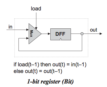
1-位寄存器:
/**
 * 1-bit register:
 * If load[t] == 1 then out[t+1] = in[t]
 *                 else out does not change (out[t+1] = out[t])
 */

CHIP Bit {
    IN in, load;
    OUT out;

    PARTS:
    Mux(a= out1, b=in,  sel=load, out=out2);
    DFF(in=out2, out=out1, out=out);
}
寄存器:由1-位寄存器来构建w-位寄存器是非常简单的。所需要做的就是构建一组w比特门,然后将寄存器的load输入赋予每个门。
CHIP Register {
    IN in[16], load;
    OUT out[16];

    PARTS:
    Bit(in=in[0], load=load, out=out[0]);
    Bit(in=in[1], load=load, out=out[1]);
    Bit(in=in[2], load=load, out=out[2]);
    Bit(in=in[3], load=load, out=out[3]);
    Bit(in=in[4], load=load, out=out[4]);
    Bit(in=in[5], load=load, out=out[5]);
    Bit(in=in[6], load=load, out=out[6]);
    Bit(in=in[7], load=load, out=out[7]);
    Bit(in=in[8], load=load, out=out[8]);
    Bit(in=in[9], load=load, out=out[9]);
    Bit(in=in[10], load=load, out=out[10]);
    Bit(in=in[11], load=load, out=out[11]);
    Bit(in=in[12], load=load, out=out[12]);
    Bit(in=in[13], load=load, out=out[13]);
    Bit(in=in[14], load=load, out=out[14]);
    Bit(in=in[15], load=load, out=out[15]);
}
内存(Memories):可以通过将寄存器堆叠起来形成随机存取存储器(random access memory, RAM)。在RAM上能够随机访问被选择的字而不会受限于访问顺序,即随机存取存储器中的任何字都能以相等的速度被直接访问。
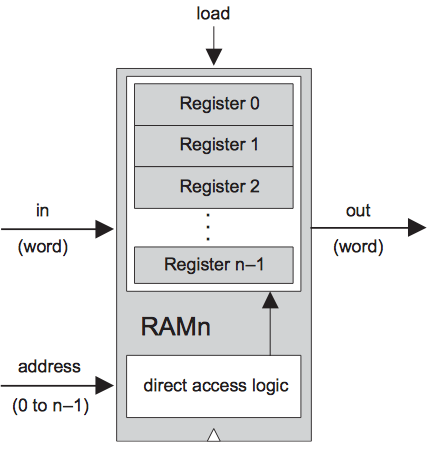
RAM8:
/**
 * Memory of 8 registers, each 16 bit-wide. Out holds the value
 * stored at the memory location specified by address. If load==1, then
 * the in value is loaded into the memory location specified by address
 * (the loaded value will be emitted to out from the next time step onward).
 */

CHIP RAM8 {
    IN in[16], load, address[3];
    OUT out[16];

    PARTS:
    // Put your code here:
    DMux8Way(in=load, sel=address, a=loada, b=loadb, c=loadc, d=loadd, e=loade, f=loadf, g=loadg, h=loadh);
    Register(in=in, load=loada, out=outa);
    Register(in=in, load=loadb, out=outb);
    Register(in=in, load=loadc, out=outc);
    Register(in=in, load=loadd, out=outd);
    Register(in=in, load=loade, out=oute);
    Register(in=in, load=loadf, out=outf);
    Register(in=in, load=loadg, out=outg);
    Register(in=in, load=loadh, out=outh);
    Mux8Way16(a=outa, b=outb, c=outc, d=outd, e=oute, f=outf, g=outg, h=outh, sel=address, out=out);
}
RAM64:
/**
 * Memory of 64 registers, each 16 bit-wide. Out holds the value
 * stored at the memory location specified by address. If load==1, then
 * the in value is loaded into the memory location specified by address
 * (the loaded value will be emitted to out from the next time step onward).
 */

CHIP RAM64 {
    IN in[16], load, address[6];
    OUT out[16];

    PARTS:
    DMux8Way(in=load, sel=address[3..5], a=loada, b=loadb, c=loadc, d=loadd, e=loade, f=loadf, g=loadg, h=loadh);
    RAM8(in=in, load=loada, address=address[0..2], out=outa);
    RAM8(in=in, load=loadb, address=address[0..2], out=outb);
    RAM8(in=in, load=loadc, address=address[0..2], out=outc);
    RAM8(in=in, load=loadd, address=address[0..2], out=outd);
    RAM8(in=in, load=loade, address=address[0..2], out=oute);
    RAM8(in=in, load=loadf, address=address[0..2], out=outf);
    RAM8(in=in, load=loadg, address=address[0..2], out=outg);
    RAM8(in=in, load=loadh, address=address[0..2], out=outh);
    Mux8Way16(a=outa, b=outb, c=outc, d=outd, e=oute, f=outf, g=outg, h=outh, sel=address[3..5], out=out);
}
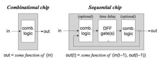
计算机芯片分为两种:组合芯片(combinational chip)和时序芯片(sequential chip or clocked chip时钟芯片)。组合芯片的操作具有即时性(instantaneous)。时序芯片的操作受时钟控制,输入的改变只有在下一个时钟周期才反应到芯片的输出管脚上: out(t)=out(t-1)。
计数器(Counter): 计数器是一种时序芯片,它的状态是整数,每经过一个时间周期,该整数就增加1个单位,执行函数out(t)=out(t-1)+c,这里就是1。典型的CPU包括一个程序计数器(program couter, PC),它的输出是当前程序中下一步将要执行的指令地址。
w-位计数器包含两个主要部分:一个常规的w-位寄存器和组合逻辑。组合逻辑用来:(a)执行计数功能;(b)根据控制位的3种不同的命令值,将计数器置于正确的操作模式。
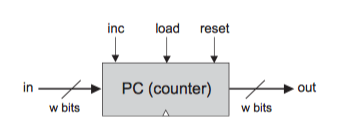
/**
 * A 16-bit counter with load and reset control bits.
 * if      (reset[t] == 1) out[t+1] = 0
 * else if (load[t] == 1)  out[t+1] = in[t]
 * else if (inc[t] == 1)   out[t+1] = out[t] + 1  (integer addition)
 * else                    out[t+1] = out[t]
 */

CHIP PC {
    IN in[16],load,inc,reset;
    OUT out[16];

    PARTS:
    Inc16(in=regout, out=plusone);
    Mux16(a=false, b=plusone, sel=inc, out=incout);
    Mux16(a=incout, b=in, sel=load, out=loadout);
    Mux16(a=loadout, b=false, sel=reset, out=toload);
    Or(a=load, b=reset, out=loadorreset);
    Or(a=loadorreset, b=inc, out=loadflag);
    Register(in=toload, load=loadflag, out=regout);
    Or16(a=regout, b=regout, out=out);
}
4 机器语言
机器语言用来对底层程序进行编码,从而形成一系列机器指令。应用这些指令,程序员可以命令处理器执行算数和逻辑餐座,在内存中进行存取操作,让数据在寄存器之间传递,验证布尔表达式的值,等等。机器语言的设计目标是直接运行在指定的硬件平台上,能够对这个平台进行全面操控;与机器语言相反,高级语言具有通用性和较强的表达能力。
机器语言是整个计算机题系统意义最深奥的接口 -- 它也是硬件和软件相接的中间线。因此,既可以将机器语言看作编程工作,也可以将其看作硬件平台内部不可分割的一部分。
5 计算机体系结构
存储程序的概念:指令没有被嵌入到硬件中,而是被存储在计算机的存储设备(memory)里,当计算机载入不同的程序指令时,同样的硬件平台可以实现不同的功能。
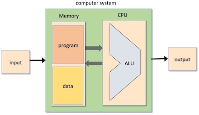
冯·诺依曼体系结构(概念上的): 冯·诺依曼体系结构的基础是一个中央处理单元(CPU),它与内存进行交互,负责从输入设备接收数据,向输出设备发送数据。
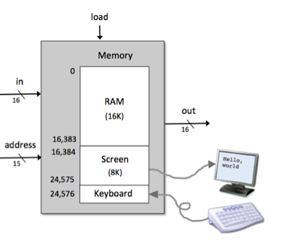
RAM: RAM不光存储数据和指令,还可以通过内存映像(Memory Maps)在CPU和计算机输入/输出设备之间充当接口。下图中屏幕和键盘都通过内存映像与计算机平台进行接口。
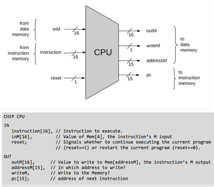
CPU包括执行指令的ALU、一组寄存器和一些用于取指令和对指令解码的控制逻辑。用来执行下面的任务:
- 指令解码(Instruction decoding):解析出指令所代表意思(指令的功能)。
- 指令执行(Instruction execution):发信号指示计算机的各个部分应该做什么工作来执行指令(指令的功能)。
- 读取下一条指令(Next instruction fetching):指出下一步执行哪一条指令(指令的功能以及ALU的输出)。